Repairing a laptop motherboard at the chip level isn’t guesswork—it’s a structured process that depends heavily on accurate technical documentation. If you’re working on the Lenovo ThinkPad Z61, one resource stands out above the rest: the BW2 schematic diagram. Without it, even experienced technicians can waste hours tracing signals blindly or misdiagnosing faults.
Let’s break down why this schematic is so essential and how it can significantly improve your repair workflow.
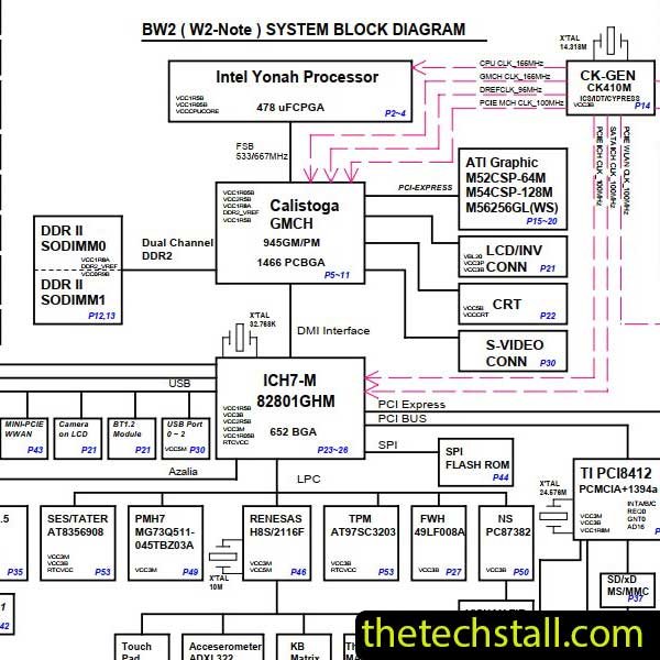
The BW2 schematic diagram is essentially the blueprint of the Lenovo ThinkPad Z61 motherboard. It shows how every component—resistors, capacitors, ICs, coils, and connectors—is interconnected. When dealing with issues like no power, no display, or charging faults, this level of detail becomes critical.
Instead of relying on trial and error, the schematic allows you to:
For example, if the laptop is not powering on, the schematic helps you follow the power rail from the DC jack through the charging IC and into the system power circuits. This eliminates guesswork and reduces repair time.
Chip-level repairing demands precision. The BW2 schematic diagram gives you access to exact component values and circuit logic, making it easier to diagnose:
Instead of replacing multiple components unnecessarily, you can pinpoint the exact fault. This not only saves time but also improves your success rate and professionalism as a technician.
Modern laptop motherboards follow a strict power-on sequence. If even one signal fails, the system won’t boot. The BW2 schematic diagram clearly outlines these sequences, including:
By referencing these signals, you can determine exactly where the sequence is breaking down. This is especially useful when dealing with “dead board” cases.
Another major advantage of using the BW2 schematic diagram is the ability to identify exact component specifications. You’ll find:
This is crucial when replacing damaged or missing components. Without this information, you risk installing incorrect parts, which can cause further damage.
While the BW2 schematic diagram is powerful on its own, combining it with other tools and resources can elevate your repair efficiency:
Boardview software allows you to visually locate components on the motherboard. When used alongside the schematic, it becomes much easier to map theory to actual hardware.
A digital multimeter helps verify voltages and continuity, while an oscilloscope is useful for analyzing clock signals and waveforms referenced in the schematic.
Sometimes the issue lies in corrupted firmware. Having access to the correct BIOS file for the BW2 board is essential for complete diagnostics.
The schematic lists IC part numbers, but datasheets give deeper insight into how those chips function. This helps when troubleshooting complex circuits like charging or CPU power sections.
Imagine you’re dealing with a Lenovo ThinkPad Z61 that shows no signs of life. Using the BW2 schematic diagram, you can:
This structured approach can turn a “dead board” into a successful repair in significantly less time.
You can access and download the BW2 schematic diagram for free using the link below:
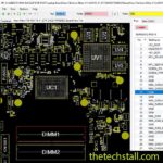
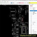
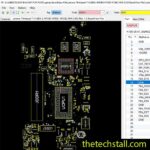
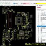
Download “Lenovo ThinkPad Z61 BW2 Rev 3B Schematic Diagram” view – Downloaded 373 times – 78.33 KBFor any technician working on Lenovo ThinkPad Z61 laptops, the BW2 schematic diagram isn’t optional—it’s essential. It transforms your repair process from guesswork into a logical, efficient workflow. Whether you’re diagnosing power issues, replacing components, or analyzing signal flow, this schematic provides the clarity you need.

For tips on chip-level repair of laptop and desktop motherboards, visit our YouTube channel Repair Assistant and subscribe to our Facebook page repairassiastantbd for repair resource updates.
When combined with boardview files, proper tools, and reliable repair resources, it becomes a complete solution for chip-level motherboard repairing.