For laptop motherboard technicians working at the chip level, precision is everything. When dealing with Lenovo K26 model, one document becomes absolutely essential: the NAU00 LA-6101P schematic diagram. Without it, troubleshooting becomes guesswork. With it, diagnosis becomes structured, logical, and efficient.
In today’s competitive repair industry, speed and accuracy determine profitability. Whether you’re operating an independent repair lab or managing a professional service center, understanding how to properly use the NAU00 LA-6101P schematic diagram can significantly improve your repair workflow.
Let’s break down why this schematic is such a powerful tool for chip-level motherboard repair.
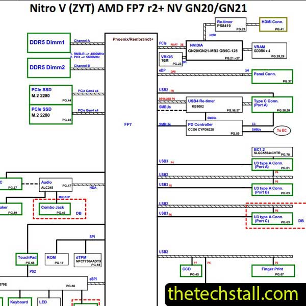
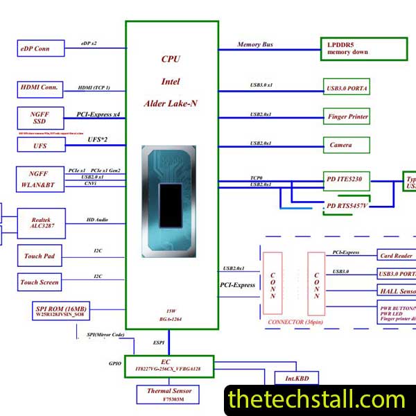
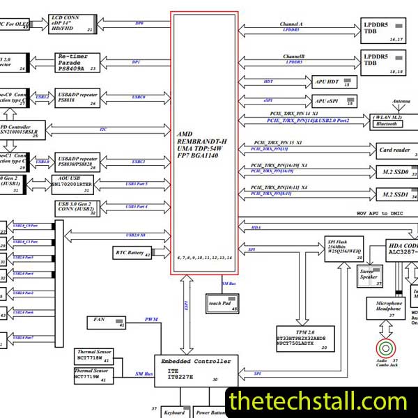
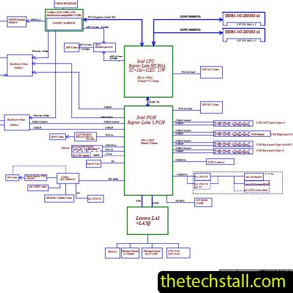
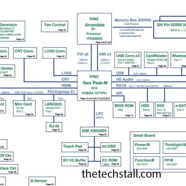
The Lenovo K26 series are widely used in corporate and educational environments worldwide. These laptops are built on the NAU00 LA-6101P motherboard platform, which integrates Intel CPU architecture, PCH chipset, Memory circuits, charging ICs, BIOS, EC (Embedded Controller), and various power rails.
At chip level, failures typically occur in:
Without the NAU00 LA-6101P schematic diagram, tracing these circuits manually on the board is extremely time-consuming. The schematic transforms complex multilayer board layouts into understandable circuit flows.
One of the most common motherboard issues is “No Power” or “No Display.” The NAU00 LA-6101P schematic diagram allows technicians to:
Instead of randomly injecting voltage or removing components, you can systematically check the power sequence from adapter input to CPU core.
Short circuits are common in Lenovo K26 motherboards. Using the NAU00 LA-6101P schematic diagram, technicians can:
This significantly reduces board damage risk caused by blind voltage injection.
Modern laptops rely heavily on signal integrity. A missing clock signal, reset signal, or BIOS communication line can completely prevent boot.
With the NAU00 LA-6101P schematic diagram, you can:
Signal tracing becomes logical rather than experimental.
At chip level, replacing the correct component is critical. The schematic provides:
For example, if a charging IC fails, the NAU00 LA-6101P schematic diagram helps you verify:
This eliminates unnecessary part replacements.
Many technicians struggle not because they lack skill, but because they lack structured diagnosis. The NAU00 LA-6101P schematic diagram converts random troubleshooting into a step-by-step process:
This systematic flow dramatically improves repair success rates.
While the schematic is powerful, combining it with other resources makes repair even more efficient.
A boardview file works alongside the NAU00 LA-6101P schematic diagram to show the physical location of components on the motherboard. While the schematic explains circuit logic, the boardview tells you exactly where to probe or replace components.
Using both together reduces time spent searching for tiny SMD parts.
BIOS corruption is common in these models. Keeping clean BIOS dump files allows you to:
The schematic helps you locate the BIOS chip and verify SPI communication lines.
Embedded Controller (EC) failures can stop the power sequence entirely. Using proper EC programming tools along with schematic reference ensures:
The NAU00 LA-6101P schematic diagram becomes even more powerful when used with:
The schematic tells you what should happen. Your tools confirm whether it is happening.
In today’s global laptop repair industry, customers expect quick turnaround times and reliable repairs. By mastering the NAU00 LA-6101P schematic diagram, technicians can:
Accurate diagnosis not only saves time but also builds long-term trust with clients.
You can download the NAU00 LA-6101P schematic diagram here:
Download “Lenovo K26 LA-6101P NAU00 Rev 1.0 schematic” Lenovo-K26-LA-6101P-NAU00-Rev-1.0-schematic.zip – Downloaded 288 times – 1.06 MBFor any technician working on Lenovo K26 laptops, the NAU00 LA-6101P schematic diagram is not optional — it is essential. It transforms complex chip-level motherboard repair into a structured, fast, and highly accurate process.
When combined with boardview files, BIOS dumps, EC firmware tools, and proper diagnostic equipment, this schematic becomes the backbone of professional motherboard repair.
If you’re serious about improving your chip-level troubleshooting skills and increasing your repair success rate, having access to the NAU00 LA-6101P schematic diagram is a must.

For tips on chip-level repair of laptop and desktop motherboards, visit our YouTube channel Repair Assistant and subscribe to our Facebook page repairassiastantbd for repair resource updates.
This may be your best resource for fixing laptop motherboard chiplevel faults.