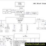
For laptop motherboard technicians working at the chip level, having access to the right schematic can make the difference between a quick fix and hours of guesswork. The HEDWIG02-6050A3285801-MB-A01 Schematic Diagram is an essential resource when repairing the HP 240 G8 motherboard, offering detailed insights into circuit paths, voltage rails, and component layouts. This guide walks you through how to effectively use this schematic to diagnose and repair common chip-level issues.
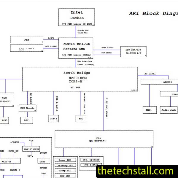
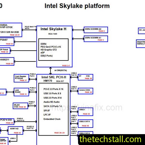
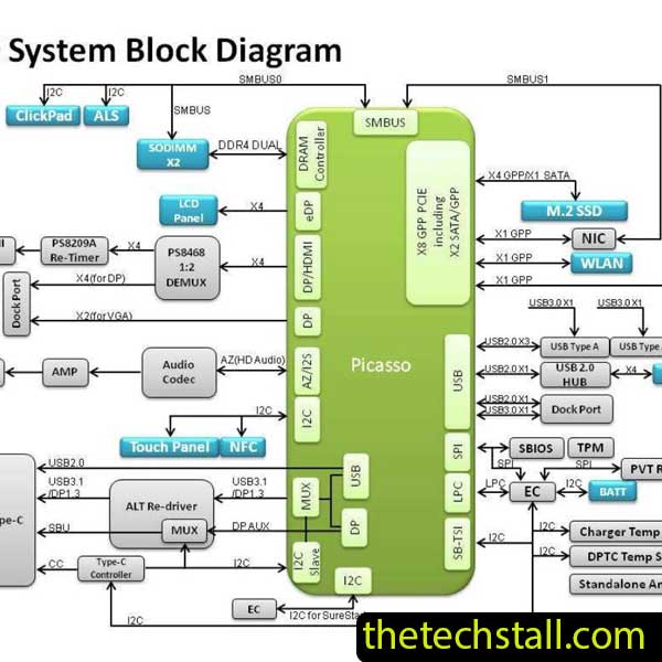
Before diving into repairs, it’s worth understanding why the HEDWIG02-6050A3285801-MB-A01 Schematic Diagram is so valuable. Unlike boardview files, which mainly show component placement, schematics reveal how each component is electrically connected. This allows technicians to trace signals, identify faulty components, and understand the board’s behavior under different conditions.
For the HP 240 G8, common issues like no power, no display, or charging failures often stem from faults in power management circuits, BIOS chips, or embedded controller (EC) sections. The schematic provides a roadmap to locate and test these areas accurately.
When working on this model, technicians frequently encounter:
Using the HEDWIG02-6050A3285801-MB-A01 Schematic Diagram, you can systematically approach each problem rather than relying on trial and error.
Begin by identifying the main power rails in the schematic, such as +3VALW, +5VALW, and CPU core voltages. Use a multimeter to check whether these voltages are present on the board.
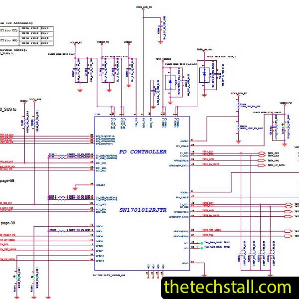
If a rail is missing, trace it back using the HEDWIG02-6050A3285801-MB-A01 Schematic Diagram to locate the responsible IC or MOSFET. This helps narrow down the faulty section quickly.
Short circuits are a common issue in chip-level repairs. Use the schematic to identify capacitors and coils connected to the affected rail. Inject voltage carefully and monitor heat generation to pinpoint the faulty component.
The schematic ensures you’re injecting voltage at the correct point and not damaging sensitive components.
If the board powers on but shows no display, the BIOS or EC may be the culprit. The HEDWIG02-6050A3285801-MB-A01 Schematic Diagram helps locate the BIOS chip and its supporting circuitry, including resistors and power lines.
Reflashing or replacing the BIOS becomes much easier when you understand its exact connections.
For issues like no display or USB failure, signal tracing is essential. The schematic allows you to follow data lines between chips, ensuring continuity and proper signal flow.
This is especially useful when dealing with chipset or CPU-related faults.
While the schematic is your primary map, experienced technicians know that a map is better when paired with a “satellite view.” To master the HEDWIG02-6050A3285801-MB-A01 motherboard, you should use these resources in tandem:
One of the most common mistakes is replacing chips without checking the power sequence. The HEDWIG02-6050A3285801-MB-A01 Schematic Diagram often includes a power-up sequence chart. This chart tells you the chronological order in which voltages must appear. If $+3.3V\_ALW$ is present but $+1.0V\_PCH$ is missing, you know exactly where the “break” in the chain is located.

For tips on chip-level repair of laptop and desktop motherboards, visit our YouTube channel Repair Assistant and subscribe to our Facebook page repairassiastantbd for repair resource updates.
The HP 240 G8 is widely used, making it a common device on repair benches worldwide. Having access to the HEDWIG02-6050A3285801-MB-A01 Schematic Diagram allows technicians to handle repairs more confidently and professionally. It reduces diagnostic time, minimizes guesswork, and increases repair success rates.
To support technicians, you can access the HEDWIG02-6050A3285801-MB-A01 Schematic Diagram through the link below:
Download “HP 240 G8 HEDWIG02-6050A3285801-MB-A01 Schematic Diagram” view – Downloaded 818 times – 82.62 KBIf you’re serious about improving your chip-level repair skills, working alone will slow you down. That’s why joining a dedicated repair network makes a real difference.
Our community at:
👉 https://repaircommunity.thetechstall.com/
Gives you access to:
Instead of wasting hours searching for a single repair resource file in different places, join our repair community for free and request the file you want. Our tech support team will try to deliver it as quickly as possible. This is an effective way to improve quickly.
Mastering chip-level repair on the HP 240 G8 requires patience, the right tools, and, most importantly, accurate information. By following the HEDWIG02-6050A3285801-MB-A01 Schematic Diagram, you move away from “trial and error” and toward “scientific diagnosis.” This not only saves you time but also prevents further damage to the customer’s hardware.
Are you ready to start your repair? Access the essential documents top to get your bench ready for the next HP 240 G8 that walks through your door.
By combining it with tools like boardview files, datasheets, and BIOS resources, you can handle even the toughest repair challenges with confidence.