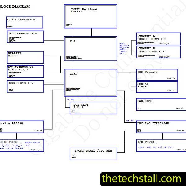
The Gigabyte GA-P31-DS3L is a popular choice among budget-conscious PC builders for its robust performance and reliability. However, like any piece of hardware, it can experience issues that may require advanced troubleshooting. For those diving into chip-level repairs, understanding the GA-P31-DS3L Rev 1.0&1.1 schematic diagram is essential. In this guide, we’ll break down how the schematic diagram works and its importance in diagnosing and repairing this motherboard.
A schematic diagram is a detailed representation of the electrical connections and components within a device. For the GA-P31-DS3L Rev 1.0&1.1 motherboard, it maps out the layout and interactions of crucial elements like:
This visual blueprint is indispensable for chip-level repairs as it helps technicians understand the electrical flow and pinpoint faults effectively.
The schematic diagram identifies every chip, resistor, and capacitor on the motherboard. Knowing which component controls specific functions (e.g., power delivery, audio processing) allows technicians to troubleshoot with precision.
The diagram maps signal pathways, enabling you to track where a failure might occur. For instance, if the USB ports aren’t functioning, the schematic can show you where the signal flow might be disrupted.
Using the diagram alongside a multimeter, you can measure voltages at various points to diagnose issues like:
If a component is damaged, the schematic provides details such as part numbers and specifications. This ensures proper replacements are used.
Every schematic uses a standard set of symbols for components. For instance:
Motherboards rely on multiple power rails (e.g., +12V, +5V, +3.3V). The schematic shows how these are distributed and regulated. Issues here often lead to startup failures or instability.
The schematic divides the motherboard into sections, such as:
Work systematically within these blocks to isolate the fault.
Many schematics include test points—locations where you can measure voltages or signals. Use a multimeter or oscilloscope to verify functionality.
To make full use of the GA-P31-DS3L Rev 1.0&1.1 schematic, ensure you have these tools:
You can open the downloaded file using Free PDF Reader & Viewer Software.
The GA-P31-DS3L Rev 1.0&1.1 schematic diagram is your gateway to successful chip-level repairs on the Gigabyte GA-P31-DS3L motherboard. By mastering how to read and interpret this blueprint, you can diagnose and fix even the most complex hardware issues.
Whether you’re a seasoned technician or an enthusiastic DIYer, investing time in understanding the schematic will save you hours of frustration and help you bring life back to faulty motherboards.
Share with friends