HP DV6 UP6/UP7 DA0UP6MB6F0 Schematic Diagram

HP DV6 UP6/UP7 DA0UP6MB6F0 Schematic Diagram

Get the free UP6/UP7 DA0UP6MB6F0 PDF and learn the important role of the DA0UP6MB6F0 schematic diagram in chip-level repairs for HP DV6 laptop motherboards.

If you’re passionate about laptop repairs or a technician looking to elevate your skills, having the right resources is essential. For anyone working on HP DV6 laptop motherboards, the DA0UP6MB6F0 schematic diagram is a game-changer. In this blog post, we will learn why this schematic is important for chip-level repairs and how you can get the free UP6/UP7 DA0UP6MB6F0 PDF to simplify your repair tasks.

Why the UP6/UP7 DA0UP6MB6F0 Schematic Diagram Is a Must-Have

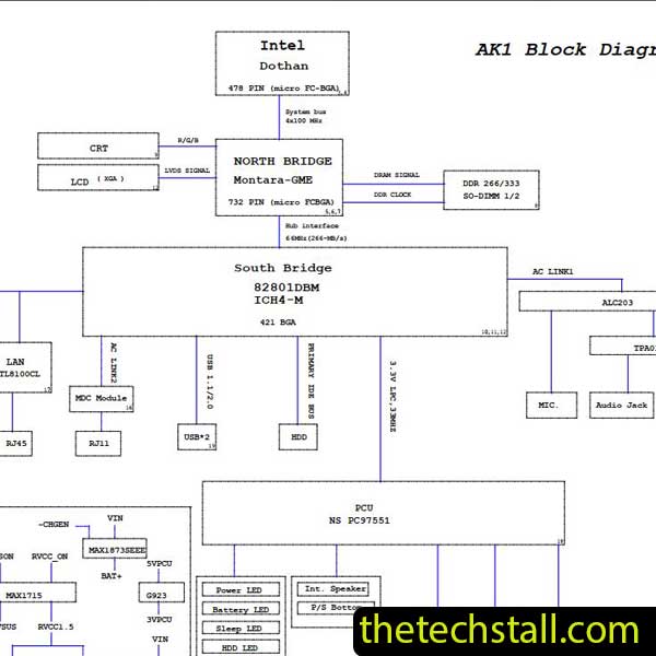
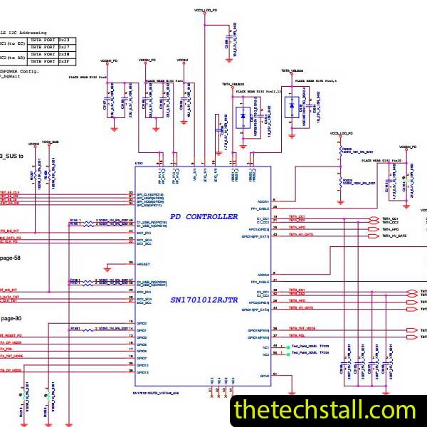
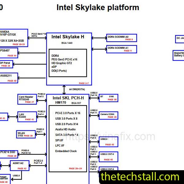
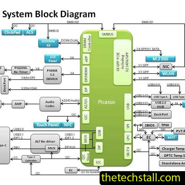
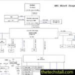
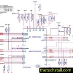
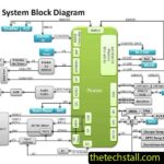
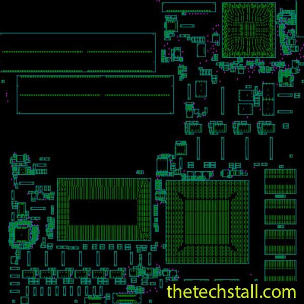
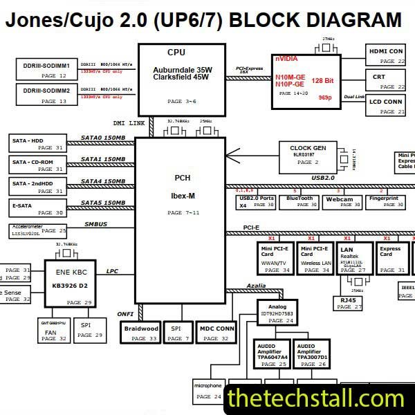
The UP6/UP7 DA0UP6MB6F0 schematic diagram provides a detailed map of the circuits, components, and connections that make up the HP DV6 motherboard. Here’s why it’s invaluable:

  1. Accurate Troubleshooting
    Identifying faulty components at the chip level can be daunting without a clear guide. The schematic diagram outlines the motherboard’s layout, helping you pinpoint the exact source of issues such as no power, no display, or component failures.
  2. Efficient Repairs
    With the UP6/UP7 DA0UP6MB6F0 schematic, you can reduce trial-and-error during repairs. It provides a clear understanding of voltage points, signal pathways, and critical IC configurations.
  3. Learning Opportunity
    For aspiring technicians, the schematic is a goldmine for learning how laptop motherboards function. It introduces you to the interplay between chips, capacitors, resistors, and other micro-components.

Key Features of the DA0UP6MB6F0

The schematic diagram for the HP DV6 motherboard includes:

  • Detailed circuit diagrams for essential chips and components.
  • Power delivery routes to diagnose power-related issues.
  • Signal pathways for debugging input/output errors.
  • Component references to locate parts efficiently on the physical board.

These features make the UP6/UP7 DA0UP6MB6F0 PDF an essential tool for professional technicians and DIY enthusiasts alike.

Practical Applications of the UP6/UP7 DA0UP6MB6F0 Schematic

Once you have the schematic, here’s how to use it effectively:

  • Diagnose Faulty Components: Check for short circuits, missing voltages, or damaged ICs.
  • Understand Power Flow: Use the diagram to trace the power delivery from the adapter to the motherboard components.
  • Learn Component Placement: Familiarize yourself with the layout to quickly locate resistors, capacitors, and other small parts.

How to Get the Free UP6/UP7 DA0UP6MB6F0 PDF

Luckily, you can now download the UP6/UP7 DA0UP6MB6F0 schematic diagram for free. Download and save the PDF file for offline use during your repair project. Foxit PDF Reader will help you open the PDF file.

Download “HP DV6 UP6/UP7 DA0UP6MB6F0 Schematic Diagram” view – Downloaded 49 times – 91.29 KB

The DA0UP6MB6F0 schematic diagram is a critical tool for anyone working on the HP DV6 motherboard. It not only streamlines repairs but also enhances your understanding of chip-level diagnostics. By downloading the free UP6/UP7 DA0UP6MB6F0 PDF, you’re taking the first step toward mastering complex laptop repairs.

Get your hands on this invaluable resource today and repair with confidence! The files in the link below are very helpful in performing chiplevel repair more efficiently.

Share with friends

Leave a Reply

Your email address will not be published. Required fields are marked *

Related Post