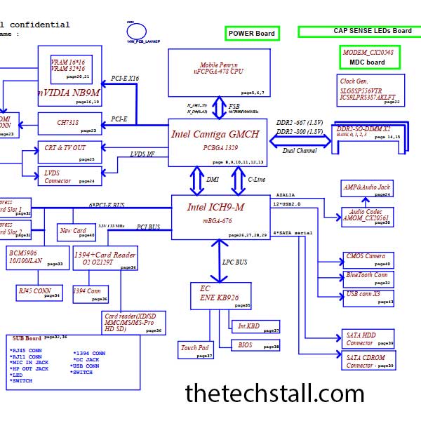
If you work in the global laptop chip-level repairing industry, you already know that motherboard repair is not guesswork—it’s precision engineering. And when it comes to repairing the Lenovo Ideapad Y430, one file can save hours of troubleshooting: the LA-4141P Schematic Diagram.
For professional laptop motherboard technicians, having the right schematic isn’t just helpful—it’s critical. In this guide, we’ll explore why downloading the LA-4141P Schematic Diagram is essential, how it improves repair efficiency, and what additional repair resources you should use alongside it.
Let’s dive in.
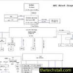
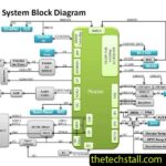
A schematic diagram is a detailed electrical blueprint of the motherboard. It shows:
Unlike a boardview file, a schematic explains how components are electrically connected and how signals flow across the motherboard.
Simply put, it tells you why something is not working—not just where it is located.
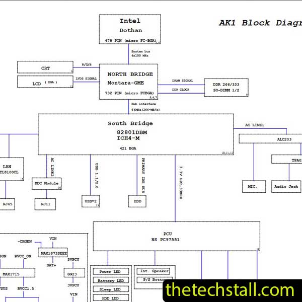
The Lenovo Ideapad Y430 is a high-performance machine. Because it handles significant power loads and generates substantial heat, its motherboard architecture is complex. Here is why the LA-4141P Schematic Diagram is non-negotiable for professional repair:
1. Pinpointing the Power Sequence
The LA-4141P uses a sophisticated power management system to transition from (19V) down to the various S5, S3, and S0 states. Without the schematic, identifying which “Always On” voltage is missing becomes a guessing game. The diagram allows you to track the Power Sequence, ensuring that the EC (Embedded Controller) is communicating correctly with the PCH and CPU.
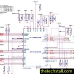
2. Identifying “Ghost” Components
Burnt components are easy to see, but what about the ones that look fine but are electrically dead? The schematic provides the exact specifications for resistors, capacitors, and MOSFETs. For example, if a buck converter fails, you need to know the exact feedback resistor values to ensure the output voltage remains stable.
3. Understanding Signal Rails
Modern laptops rely on high-speed data signals like LPC, SMBus, and I2C. If the Lenovo Ideapad Y430 is stuck on a black screen, the LA-4141P Schematic Diagram helps you probe the BIOS chip or the RAM slots to see if the reset signals (PLTRST#) are being released.
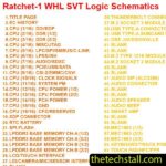
Based on global technician feedback, the LA-4141P motherboard often presents with a few recurring “Achilles heels”:
In today’s competitive repair industry, time is money. The right schematic can cut diagnostic time in half.
While the schematic is the “brain,” you need a few more “limbs” to complete a professional repair. To truly master the LA-4141P board, you should use the following resources in tandem:
Ready to get that Lenovo Ideapad Y430 back on the customer’s desk in working order? We have provided a high-quality, searchable PDF version of the motherboard logic for your convenience. Click the link below to download the LA-4141P Schematic Diagram
Chip-level repair is an art form backed by data. Every time you open a Lenovo Ideapad Y430, you are looking at millions of traces and thousands of components. The LA-4141P Schematic Diagram isn’t just a PDF; it’s your insurance policy against mistakes. It saves you time, prevents further damage to the customer’s board, and ultimately increases your shop’s “Success Rate” and profitability.
Stop guessing and start measuring. By integrating the schematic with a solid Boardview and a multimeter, you transform from a “parts swapper” into a true “motherboard engineer.”

For tips on chip-level repair of laptop and desktop motherboards, visit our YouTube channel Repair Assistant and subscribe to our Facebook page repairassiastantbd for repair resource updates.
Pro Tip: Always cross-reference the revision number on your physical motherboard (e.g., Rev 1.0 or 2.0) with the schematic version to ensure 100% accuracy during signal tracing.