In the high-stakes world of laptop chip-level repairing, information is the difference between a successful fix and a “no-fix” pile. One of the most valuable resources for technicians working on the HP Mini 5103 is the 6050A2378301-MB-A03 schematic diagram. This document provides a detailed map of the motherboard’s electrical circuits, helping technicians trace faults, identify components, and perform precise repairs. 🔧💻.
In this guide, we will explain how the 6050A2378301-MB-A03 schematic diagram helps laptop repair technicians, why it is essential for motherboard troubleshooting, and which additional repair resources can make your work easier and more efficient.
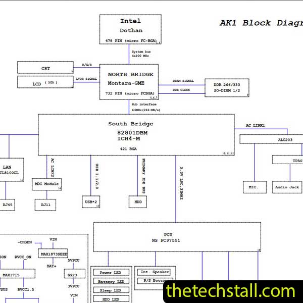
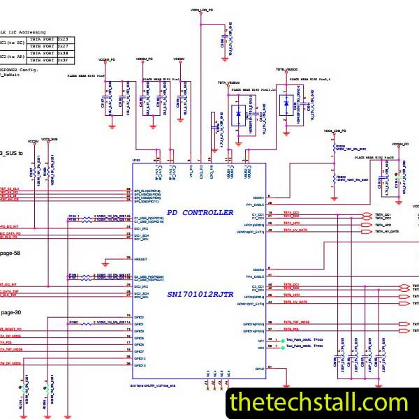
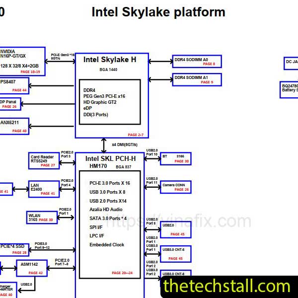
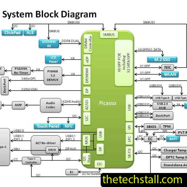
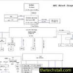
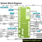
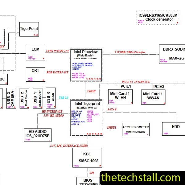
The 6050A2378301-MB-A03 schematic diagram is a technical document that represents the electrical design of the HP Mini 5103 motherboard. Instead of showing physical component placement, a schematic diagram displays how components are connected electrically.
Technicians use it to understand how signals, voltages, and circuits flow across the board.
Typical information found in the 6050A2378301-MB-A03 schematic diagram includes:
For chip-level technicians, this information is critical when diagnosing motherboard faults.
Modern laptop motherboards are extremely complex. Without a schematic, troubleshooting becomes guesswork.
Here are some key benefits of using the 6050A2378301-MB-A03 schematic diagram.
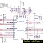
When a HP Mini 5103 fails to power on, shows no display, or shuts down randomly, the schematic allows technicians to follow the circuit step by step.
For example, you can:
This significantly speeds up the repair process.
Motherboards contain hundreds of tiny SMD components. The 6050A2378301-MB-A03 schematic diagram provides the exact component labels such as:
Once you identify the faulty component in the circuit, you can locate it on the motherboard using the boardview file or silk screen markings.
For new technicians, studying the 6050A2378301-MB-A03 schematic diagram also improves their understanding of motherboard design.
You can learn how:
This knowledge helps technicians handle more complex repairs over time. 📘
Technicians frequently use the 6050A2378301-MB-A03 schematic diagram when repairing these common faults in HP Mini 5103 laptops:
By tracing circuits and checking voltage levels, technicians can isolate the defective component and repair the board instead of replacing it.
While the 6050A2378301-MB-A03 schematic diagram is your primary map, a master technician uses a full toolkit of digital resources:
To get the most value from the 6050A2378301-MB-A03 schematic diagram, technicians should follow these practices:
✔ Always check the power sequence first
✔ Identify main power rails (3.3V / 5V)
✔ Trace signals step-by-step instead of jumping circuits
✔ Use boardview files to locate components faster
✔ Verify voltages using a multimeter before replacing parts
Following these steps can significantly increase repair success rates.
If you are repairing the HP Mini 5103 motherboard, having the correct schematic file is essential.
You can download the 6050A2378301-MB-A03 schematic diagram for free using the link below:
Download “HP Mini 5103 6050A2378301-MB-A03 Schematic Diagram” view – Downloaded 516 times – 78.35 KBIn a global market, the speed of repair determines your profitability. Using a 6050A2378301-MB-A03 schematic diagram reduces the time spent on “blind” troubleshooting and prevents accidental damage caused by probing the wrong components. Whether you are dealing with liquid damage or a dead PCH, having the correct documentation is non-negotiable.

For tips on chip-level repair of laptop and desktop motherboards, visit our YouTube channel Repair Assistant and subscribe to our Facebook page repairassiastantbd for repair resource updates.