If you work as a laptop motherboard technician, you already know that successful chip-level repair depends on accurate documentation, clear circuit understanding, and reliable repair resources. One wrong assumption can cost hours of troubleshooting. That’s why having access to the QL6 DAOQL6MB8F Schematic Diagram is considered a game-changer when repairing the HP 540/660/DV2 laptop motherboard.
Modern laptop motherboards are densely packed with multilayer circuits, tiny SMD components, and complex power rails. Visual inspection alone is no longer enough. A schematic diagram allows technicians to:
For the HP 540/660/DV2, the board design is not beginner-friendly. Without a proper schematic, even experienced technicians may struggle to isolate faults efficiently.
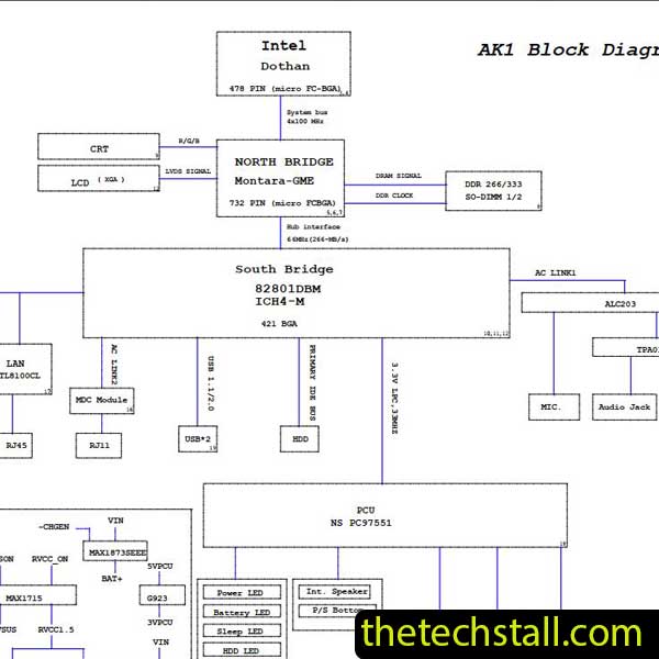
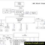
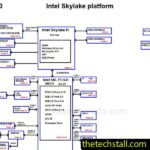
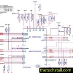
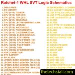
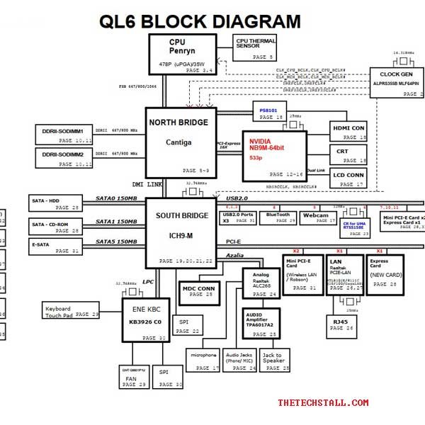
The QL6 DAOQL6MB8F Schematic Diagram provides a complete electrical blueprint of the motherboard used in the HP 540/660/DV2. It maps out every critical section, including:
With this level of detail, technicians can follow signal paths step by step, compare expected voltages, and quickly locate defective components. This significantly improves first-time repair success rates.
Many recurring motherboard problems on this model become easier to solve with the correct diagram, such as:
Instead of replacing parts randomly, technicians can test specific points referenced in the schematic and confirm the root cause before soldering.
While the schematic is the foundation, professional repair work often requires additional resources to maximize efficiency.
Boardview files complement schematics by showing physical component locations. When used together, they allow technicians to quickly identify where a component sits on the actual board.
IC datasheets provide pin definitions, voltage ranges, and functional descriptions. When matched with the schematic, datasheets help confirm whether an IC is behaving correctly.
Testing tools are essential to verify voltages, resistance values, and clock signals referenced in the schematic.
Many advanced technicians maintain voltage logs from working boards. These can be compared with schematic test points for faster fault isolation.
This schematic is especially useful for:
If you regularly repair laptop boards, this document will quickly become part of your essential toolkit.
Using the official and accurate schematic offers clear advantages:
For workshops handling multiple laptop repairs daily, these benefits translate directly into higher profitability.
To support your repair work, you can download the QL6 DAOQL6MB8F Schematic Diagram directly from the link below:
Download “HP 540 660 DV2 Quanta QL6 DAOQL6MB8F Rev2A Schematic” HP-540-DV2-Quanta-QL6-Rev-2A-Schematics.zip – Downloaded 566 times – 794.10 KBFor serious laptop motherboard technicians, working without a schematic is like repairing blindfolded. When it comes to the HP 540/660/DV2, having the right diagram is not optional—it’s essential. Combining the QL6 DAOQL6MB8F schematic diagram with boardview files, datasheets, and proper testing tools, this schematic empowers technicians to perform precise, professional-level chip-repair with confidence.

For tips on chip-level repair of laptop and desktop motherboards, visit our YouTube channel Repair Assistant and subscribe to our Facebook page repairassiastantbd for repair resource updates.