Why the N551JM Schematic Diagram Is an Essential Resource for Fixing ASUS N551JM laptop Chip-Level Motherboard Issues
In the world of laptop motherboard repair, few tools are as valuable as a precise schematic diagram. When it comes to repairing laptops—particularly the ASUS N551JM series—the N551JM schematic diagram stands out as an indispensable resource for technicians. Whether you’re an experienced chip-level engineer or just starting to explore board-level troubleshooting, understanding how to read and use this schematic can dramatically improve your diagnostic accuracy and repair success rate.
What Is the N551JM Schematic Diagram?
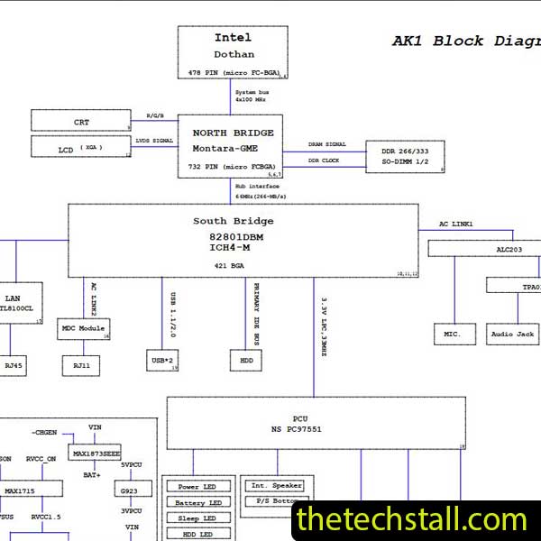
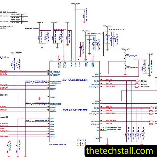
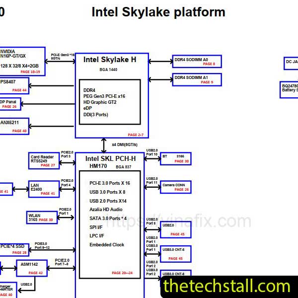
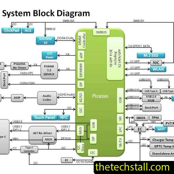
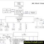
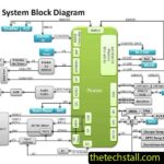
The N551JM schematic diagram is a detailed blueprint of the ASUS N551JM laptop’s motherboard. It maps every component, circuit, voltage line, and signal path used in the board’s design. From the power section and charging circuit to the CPU, GPU, and I/O controllers, this diagram provides a complete view of how different electronic components interact to make the laptop function.
Essentially, this schematic acts as the motherboard’s DNA—it allows technicians to trace issues at the microscopic level. By referencing specific voltages and component labels, engineers can quickly identify where a failure has occurred, whether it’s a shorted capacitor, burnt MOSFET, or faulty IC.
Why Every Laptop Technician Needs This Schematic
In chip-level repairing, guesswork can waste hours and lead to unnecessary part replacements. The N551JM schematic diagram eliminates that uncertainty. It gives you the information needed to:
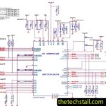
Trace Power Rails: Identify where each voltage originates and where it should be present. If the laptop doesn’t power on, you can follow the schematic to check the power sequence and find which rail is missing.
Diagnose Charging Problems: ASUS N551JM models often experience charging circuit issues. Using the schematic, you can locate the charger IC, sense resistors, and related components to verify input and output readings precisely.
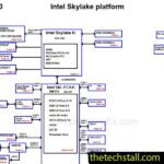
Check Signal Flow: The schematic helps in analyzing signal communication between the CPU, GPU, and memory sections. This is crucial for identifying issues like no display or system hang.
Component Replacement Accuracy: With component designators and values listed in the N551JM schematic diagram, you can replace burnt or missing parts confidently, ensuring correct ratings and compatibility.
Step-by-Step: How to Use the N551JM Schematic Diagram
Identify the Motherboard Model: Before starting, confirm that your ASUS N551JM motherboard model corresponds to N551JM. This is usually printed on the motherboard near the RAM slots or power connector.
Open the Diagram in a Viewer: Use a PDF schematic viewer to zoom in and trace the circuit areas. Start from the main power input section (DC jack) and move toward the battery charging circuit.
Follow the Power Sequence: The schematic typically begins with the adapter voltage (19V) entering through protection components like a MOSFET or fuse. Following this path step by step helps you pinpoint where voltage is lost.
Check Voltages and Signals: Use a multimeter and compare real readings with the expected voltages shown in the schematic. This direct comparison guides your troubleshooting efficiently.
Cross-reference with a Boardview File (if available): To visually locate small SMD components, pair the schematic with a matching Boardview file. Together, they provide a complete visual and functional understanding of the board layout.
Additional Repair Resources to Use with the N551JM Schematic Diagram
While the schematic itself is powerful, combining it with other professional repair tools can elevate your diagnostic accuracy:
Boardview File: The boardview shows the physical layout and component positions on the motherboard, helping you locate test points, connectors, and ICs quickly.
Datasheets for Major ICs: Refer to component datasheets for chips like the charging IC, PWM controller, or BIOS chip. These documents explain pin configurations, voltage requirements, and functionality.
Voltage and Resistance Charts: Having a reference chart for voltage and resistance values from a working motherboard can help verify your readings and spot deviations.
BIOS and EC Firmware Files: In many cases, corrupted BIOS or embedded controller firmware can cause startup failures. Always back up and, if needed, reprogram BIOS chips using verified firmware.
Why the N551JM Schematic Diagram Is a Game-Changer
For ASUS N551JM repair specialists, having access to the N551JM schematic diagram transforms repair work from guesswork into precision engineering. It saves time, reduces costs, and improves success rates on complex chip-level repairs. More importantly, it empowers technicians to provide professional-grade repair services, earning client trust and long-term satisfaction.
In today’s competitive laptop repair industry, detailed technical resources separate beginners from experts. The N551JM schematic diagram is one such resource every motherboard technician should have in their toolkit. Whether you’re diagnosing a dead board, fixing charging issues, or tracing no-display faults, this schematic provides the clarity you need to perform accurate and efficient repairs.
For tips on chip-level repair of laptop and desktop motherboards, visit our YouTube channel Repair Assistant and subscribe to our Facebook page repairassiastantbd for repair resource updates.
If you’re ready to take your ASUS N551JM motherboard repair skills to the next level, you can download the N551JM schematic diagram from the link and start mastering chip-level diagnostics today.