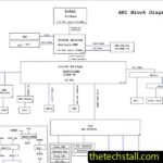
When it comes to repairing the Acer Iconia 6120 at the chip level, one essential resource stands out above all others: the PAU30 LA-6392P Schematic Diagram. For technicians dealing with motherboard faults, this document is not just a guide—it’s a map to the inner workings of the board, helping to pinpoint problems and streamline repairs.
Whether you’re an experienced repair professional or a beginner in the laptop repair field, understanding how to utilize the PAU30 LA-6392P Schematic Diagram can significantly improve your efficiency and success rate. In this post, we’ll break down how this schematic helps troubleshoot and solve chip-level issues in the Acer Iconia 6120.
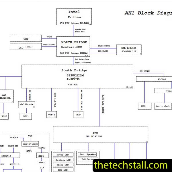
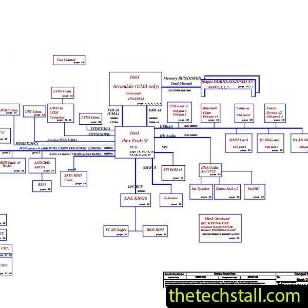
The PAU30 LA-6392P is the specific motherboard model used in the Acer Iconia 6120. The schematic diagram for this board is a detailed blueprint that shows the complete electrical design, including all components, their connections, voltage references, and signal pathways.
Think of it as a road map: instead of guessing where each trace leads or which IC controls a function, the schematic gives you direct, accurate information. It contains:
For technicians, having this information is the difference between hours of blind troubleshooting and a targeted, efficient repair.
The Acer Iconia 6120 motherboard is prone to a few recurring issues, including:
While these issues may appear similar across various laptops, chip-level repair requires identifying the exact failing component. This is where the PAU30 LA-6392P Schematic Diagram becomes critical.
Instead of manually tracing lines on the board, technicians can look up a component’s label in the schematic. For example, if the problem is with the charging circuit, you can immediately locate the charger IC and see all related resistors, capacitors, and MOSFETs.
One of the first steps in chip-level repair is checking for missing voltages. The schematic shows exactly where each voltage rail starts, which components are connected, and the expected voltage. This helps determine whether the fault is in the power generation stage or further down the line.
For issues like no display or keyboard not working, the schematic helps track signals from the source (GPU, EC, or PCH) to the destination (LCD, keyboard connector). If there’s a break or short along the path, you’ll know exactly where to probe.
Every IC in the schematic has a pin description showing its function—power input, data line, enable signal, ground, etc. This allows precise testing instead of random component replacement.
Without a schematic, diagnosing motherboard problems can turn into trial and error. With the PAU30 LA-6392P schematic, you can logically follow the circuit until you find the fault.
Imagine a technician receives an Acer Iconia 6120 that won’t turn on. The first step is to check the adapter voltage at the DC jack—it’s present. The next step is to verify voltage at the charger IC. By referring to the PAU30 LA-6392P Schematic Diagram, the technician identifies the charging chip location, its input pin, and the sequence of MOSFETs controlling power flow.
Testing with a multimeter reveals that one MOSFET gate voltage is missing, indicating a failed resistor in the gate control circuit. Without the schematic, finding that resistor could take hours. With it, the repair is completed in under 30 minutes.
In short, the schematic is both a learning tool and a professional repair resource.
[Download the PAU30 LA-6392P Schematic Diagram for Free Here]
Download “Acer Iconia 6120 PAU30 LA-6392P R1.0 Schematic Diagram” view – Downloaded 296 times – 102.56 KBThe PAU30 LA-6392P Schematic Diagram is an indispensable tool for anyone repairing the Acer Iconia 6120 motherboard at the chip level. It transforms complex fault-finding into a structured, efficient process, saving time and improving accuracy. Whether dealing with power faults, charging issues, or signal problems, this schematic gives you the knowledge to solve the problem effectively.
If you’re serious about motherboard repair, having the right schematic is non-negotiable. With the PAU30 LA-6392P diagram, you have the blueprint to restore Acer Iconia 6120 boards to working condition quickly and confidently.

For tips on chip-level repair of laptop and desktop motherboards, visit our YouTube channel Repair Assistant and subscribe to our Facebook page repairassiastantbd for repair resource updates.
So before you dive into your next fix, make sure you’ve got your tools ready—and don’t forget to grab your free PAU30 LA-6392P schematic diagram today.
You also may be interested in